Understanding PCB Materials and Specifications
by Sharad Bagri
When you give a PCB for fabrication, you need to specify details on PCB materials, impedance controls, finish, copper thickness and so on. Most of the details are so common that they are always assumed. However still it is better to know them.
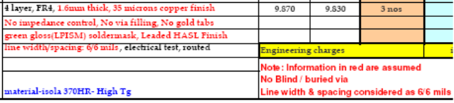
Below is a screenshot of quotation submitted by a fabricator for a PCB design of size 9.870 X 9.830 cm
Let us understand each term one by one and things related to them
1) 4 layer specifies NUMBER OF LAYERS - This means the number of conducting layers. The layers may be either routing layer or plane layer. The commonly used no. of layers are 1, 2, 4, 6, 8 and other even numbered layers. Odd number layer boards may be formed but they are not standard boards and doesn’t offer any savings. The PCB materials used for 3 or 4 layers would almost be same.
Routing layers contains tracks while plane layer are generally used to connect power or ground. Plane layers have plane of copper from which connections are drawn up or down wherever needed. Islands can be formed on plane layers and each island may have different signal. Suppose some sets of chips on one board use 3.3 V while other use 5 V then the power plane may be partitioned into two islands of 3.3 V and 5 V.
2) FR4 specifies PCB MATERIAL TYPE – FR4 is other name for “Glass reinforced epoxy laminated sheets”. It is a commonly used PCB material. The reasons for its ubiquity as a PCB material are its high dielectric strength, high mechanical strength, light weight, resistance to moisture and other properties conducive for PCB manufacturing. FR in FR4 stands for “fire retardant”, another feather in this PCB material’s cap.
3) 1.6 mm thick specifies FINISHED BOARD THICKNESS – In multilayer PCB it is thickness after all layers have been pressed together and all the processes completed. 1.6mm is default thickness for 4 layer board. Go for higher thickness if you have heavy components on board to get better strength. Keep an eye on thickness even when you have high voltages on board.
4) 35 microns copper finish – The thickness of copper put on board. Another popular way to express is in grams or Oz. (Ounces per square foot) of copper per unit area. X Oz would mean that X Ounces were spread on the Board material and it was distributed uniformly over an area of 1 square foot.
Go for higher copper thickness if the current density on board is greater than in average digital circuits. In normal boards 35 microns is good. Up till a current of 1A and copper thickness of 1 Oz, track width of 10 mils is safe.
5) No impedance Control – When signal transition time is too small or frequency is too high then tracks may behave as transmission lines. If unchecked, such tracks may cause significant power loss. For maximum power to be transferred to other end of track, length and geometry of the track should be carefully laid taking care of transmission line equations.
As a rule of thumb, if the board is of FR4 PCB material with copper tracks and signal rise time is 1 nanosecond then 2 inches is a safe distance. If the track length exceeds this and signal integrity is important then consider the transmission line effects also. There are lot of free programs and excel sheet available on net that calculate impedances for prevalent geometries. If impedance control has been mentioned to the fabricator then an extra test is done on the completed PCB to check the required impedances.
6) No Via Filling – Normally vias are not filled and you clearly see other side of the board through them. However, they can be filled for various reasons. One need arises when vias are to be protected from solutions, dust etc. Vias can also be filled with conducting materials to increase the current carrying capacity of via. One more reason is to level the board. Via filling is needed many a times on boards with BGA (Ball Grid array) components. If BGA pins make contact with one of the inner layer then the via can’t be placed just underneath the pin because then the solder may flow in the hole and get connected to some other layer. So Via filling is done so that solder doesn’t flow in the via and contacts are properly connected.
7) No gold tabs – At any place on the board when something makes and breaks contact repeatedly then that area wears out fast. Example is a rubber pushbutton which has contacts printed on the board. An example is the kind of buttons used in calculator. This wearing out also happens when daughter card slot are provided on main board. The contacts on this slot are rubbed when card is pushed in or out. In such cases it is wise to put gold layer on the surface which makes contact. This enhances life of the contact. A separate step is added in the PCB fabrication process if gold tabs are specified. Also remember gold is costly.
8) Green gloss (LPISM) soldermask - The first image that would come to your mind when you think of PCB is a green colour board with some shining metal contacts and some holes. The green colour is because of this soldermask. Now why is soldermask used?? Solder mask prevents spilling of liquid solder. This spilling has become a serious problem in recent times. As the pitch of the IC pins has decreased, due to this spilling the pins get shorted. To feel the miracle of soldermask, try to solder a board which doesn’t have solder mask (mostly a homemade PCB won’t have) and the one which has solder mask. You will feel a huge difference. This experience made me enjoy soldering which I hated earlier.
LPISM stands for Liquid Photo imageable solder mask. It is a type of soldermask. There are soldermasks available in other colours as well. Prevalent among them are Red and blue.
9) Leaded HASL finish – HASL stands for Hot Air Solder Leveling. After soldermask has been put on PCB. The PCB is passed through molten solder. All the copper which is exposed, like pads etc. get covered with solder. This is useful in actual soldering of the components. During soldering of SMD chips on board it is only needed to heat the board till solder becomes molten again and place the component at the respective position. The components get soldered as the molten solder again solidifies. No need to hold soldering guns, wires and flux. So Simple J
Leaded HASL means that lead is also present in the solder compound put on the board. Nowadays HASL compounds without lead are also available.
10) Line Width / Spacing : 6/6 mils – This means the minimum track width would be 6 mils and minimum spading between tracks, tracks and pads and all other spacings should be greater than or equal to 6 mils. In case you don’t know mils, It is the prevalent unit of distance used in PCB world. 1 mil = 1/1000th of an inch = .0254mm.
Take care of width and spacing when higher currents and voltages are expected on board.
11) Electrical test, routed – In multilayer PCB, It is not possible to do visual inspection of all the tracks for their correctness. So this test is done. Test probes are put at the end of tracks or on pads such that signals on it can be accessible. A small voltage is applied on one such probe. If that voltage is detected at the other end, it confirms that the tracks are proper. This step may not be necessary in 1 or 2 layer board but if you don’t want to compromise on quality, get this test done.
12) PCB Material-Isola 370HR-High Tg : Isola is a famous company for PCB materials and 370HR is one of their product’s name. This is an FR4 PCB material. This PCB material in addition to FR4 properties has additional advantages like superior thermal performance which helps in dissipating heat on board. The mechanical, chemical and moisture resistance properties all equal or exceed the performance of traditional FR-4 materials. “High Tg” stands for “high glass transition temperature”. This means that the PCB made of this material can sustain high temperatures. During HASL or soldering, PCBs have to sustain high temperatures and that’s where this parameter becomes important.
13) No Blind/Buried Vias – Blind Vias are those vias which join one of the outer layers (TOP or BOTTOM) with one of the inner layers. Since this via can be seen from only one side, it is called a blind via (This may not seem logical but just remember itJ). Buried vias are vias which connect one of the inner layers to another inner layer. This vias cannot be seen from any of the outer layer and hence is called buried vias. (Aha!! This is logical) Via filling as we studied above is used many a times when blind/buried vias are used. It helps level the surface just above via so that pads/tracks can be placed over the vias without the solder penetrating in.
Blind via, buried via, via filling, gold tabs put additional cost on PCB manufacturing. Also, if you go down 6 mils in line/width spacing, the cost goes up. This is because the fabrication processes change a little and also the rejection rate is high. There are PCB fabricators which can go down till 3 mils. Now some may have gone below that also, but don’t try to touch those limits until you don’t have other options.
The parameters defined above are just some of the values to define a PCB.
Top of PCB Materials and Specifications
Need More Help? Have An Opinion?
Do you need more help to solve your problem? Would you like to ask the author a question about your specific problem? Do you have a great idea about this?
We will post an answer within 2 business days. If you need more immediate assistance or you would like to discuss your issue privately, please use our contact us form or call us at 1-888-215-8557. We love solving technical issues and there is no charge if we solve your problem over email or over a short phone call.